Modern power electronics rely on discrete semiconductor topologies to convert, switch, and protect electrical energy efficiently. Understanding the foundation—from basic rectification using power rectifiers to advanced active switching using IGBTs—is essential for optimizing industrial motor drives, solar inverters, and automotive powertrains.
1. Diode Fundamentals & Rectification Topologies
Diodes form the most fundamental building block in power conversion, directing current flow and suppressing inductive switching transients.
Silicon Diode Structures Compared
┌─────────────────────────────────────────┐
│ AC Line / High-Speed │
└────────────────────┬────────────────────┘
│
┌───────────────────────────┼───────────────────────────┐
▼ ▼ ▼
Standard Rectifier Schottky Barrier Fast Recovery Diode
• High V_RRM (up to 1600V) • Low V_F (0.3V – 0.5V) • Short t_rr (<50ns – 100ns)
• Low switching frequency • Zero reverse recovery • Moderate V_F (~1.0V – 1.5V)
• Best for 50/60Hz AC line • Limited to <200V • Best for SMPS & freewheeling
- Standard Silicon Rectifiers: Designed for low-frequency (50–60Hz) mains AC rectification. They feature high repetitive peak reverse voltage (VRRM) ratings and high surge current capacity (IFSM), but exhibit slow reverse recovery times (trr).
- Schottky Barrier Diodes (SBDs): Formed by a metal-semiconductor junction rather than a P-N junction. SBDs offer extremely low forward voltage drop (VF0.30–0.50V) and virtually zero reverse recovery time, making them ideal for high-efficiency secondary-side output rectification.
- Fast & Super-Fast Recovery Diodes (FRDs): Optimized for high-frequency switching environments (>20kHz). By introducing lifetime killers (such as gold or platinum doping) into the drift region, FRDs achieve fast reverse recovery times (trr<50ns), suppressing switching energy losses (Erec) and mitigating EMI.
2. P-N Junction Physics: Reverse Recovery Characteristics
When a forward-biased P-N diode transitions to a reverse-blocking state, minority carriers accumulated in the intrinsic drift region must be cleared before the depletion layer can re-form.
ReverseRecoveryTime(trr)=ta+tb
- ta: Time taken to sweep out stored minority carriers from the junction.
- tb: Time required for the reverse current to decay back to zero (or 10% of peak reverse current IRM).
During trr, a transient reverse peak current (IRM) flows through the device. The product of IRM and the rising reverse voltage across the diode generates dynamic switching losses (Psw=VRIRMfsw), stressing both the diode and the opposing active power switch (e.g., MOSFET or IGBT) in a half-bridge topology.
3. IGBT Foundations: Combined MOSFET & BJT Advantages
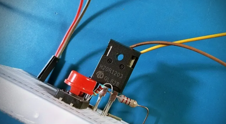
The Insulated-Gate Bipolar Transistor (IGBT) combines the high input impedance and simple voltage-controlled gate drive of an N-channel MOSFET with the low conduction loss and high current density of a PNP Bipolar Junction Transistor (BJT).
Equivalent Electrical Circuit
Collector (C)
│
▼
┌─────┐
│ PNP │
└─────┘
▲ │
│ │
┌────┴────┴────┐
│ N-MOSFET │
└──────┬───────┘
│
Gate (G)
│
Emitter (E)
Key Performance Metrics
- Saturation Voltage (VCE(sat)): The conduction voltage drop across the collector-emitter terminals during the ON state. Conductivity modulation in the N- drift region keeps VCE(sat) low (1.5V–2.2V) even under hundreds of amperes of continuous current.
- Turn-Off Tail Current: During turn-off, after the MOS gate channel closes, trapped minority carriers in the PNP base region decay slowly through recombination. This produces a “tail current,” which accounts for the majority of the IGBT’s turn-off switching loss (Eoff).
4. IGBT Market Trends & Sourcing Strategies
Understanding technology developments and market dynamics helps engineers and procurement teams optimize system reliability and sourcing costs. A comprehensive IGBT guide outlines current technology roadmaps and strategic procurement considerations.
Key Technological Trends
- Field-Stop (FS) & Trench-Gate Topologies: Modern IGBTs are shifting from legacy Punch-Through (PT) and Non-Punch-Through (NPT) structures to Field-Stop Trench technology. The vertical trench gate eliminates JFET resistance, while the thin wafer structure with a field-stop layer reduces both VCE(sat) and turn-off tail current.
- Wide-Bandgap Coexistence: While Silicon Carbide (SiC) MOSFETs are expanding in high-frequency (>100kHz), high-voltage power converters, Silicon IGBTs remain the cost-effective, dominant choice for high-power applications operating in the 1kHz–50kHz switching window.
- Module Integration: Demand is shifting from discrete packages (TO-247, TO-247GE) to integrated Intelligent Power Modules (IPMs). IPMs combine co-packaged antiparallel fast-recovery diodes, gate driver ICs, and thermal protection sensors within a single isolated substrate.
See also: Market Research Platform Strategies for Better Business Intelligence
Strategic Sourcing Considerations
IGBT Selection Criteria
┌─────────────────────────────────────────────────────────────────┐
│ System Voltage (V_DC) → Block Margin (V_CES ≥ 1.35 * V_DC) │
├─────────────────────────────────────────────────────────────────┤
│ Thermal Budget → Package R_θJC (TO-247 vs. IPM Module) │
├─────────────────────────────────────────────────────────────────┤
│ Fault Protection → Short-Circuit Safe Operating Area │
└─────────────────────────────────────────────────────────────────┘
When evaluating IGBT vendors and sourcing supply chains:
- De-rate Voltage Ratings: Ensure the collector-emitter voltage (VCES) is rated at least $30\%\text{–}40\%$ above the steady-state DC bus voltage to withstand inductive turn-off voltage spikes (Ldidt).
- Short-Circuit Ruggedness (SCWT): For motor drive applications, select IGBTs rated for a minimum $5\mu\text{s}\text{–}10\mu\text{s}$ Short-Circuit Withstand Time to allow drive electronics to detect overcurrent conditions and trigger safe shutdown sequences.
- Dual-Sourcing Strategy: Verify package footprint compatibility (standard pinouts like TO-247 and standard 62mm module housings) across secondary suppliers to insulate against supply chain disruptions and long lead times.